ADC/DAC Breakout Board
The ADC and DAC chips chosen for this project are not the most common, it seems that there are no cheap breakout boards on the market. So I’ll have to make my own!
The circuit I designed basically provides a master clock for the ADC and DAC, as well as headers to connect the RPi to the I2S lines, as well as the digital IO pins of either IC.
(See my github repo for KiCAD project files!)
Overview
The ADC and DAC both deal with the I2S audio format. This allows for efficient sending/receiving of digital audio at a constant data rate.
The Pi Zero 2 W has a PCM (Pulse-Code Modulation) peripheral; I2S is a protocol based on pulse-code modulation, and so the RPi’s peripheral is able to send and receive audio in this format.
The Texas Instruments PCM1863 ADC, the chip chosen for this project, is a masterpiece (as are most of TI’s chips; I truly love the stuff they cook up). It has two high-quality ADCs (for stereo audio), as well as an 8 channel input mux, a secondary ADC which probes the other inputs on the MUX, a DSP unit which applies configurable low-pass, high-pass, and decimation filtering to the digitized signal, as well as a few more bits and bobs here and there. It is able to derive an internal high-frequency clock for the DSP and ADC sampling from a slower I2S Clock signal.
Because of that last detail, I hoped I would be able to hook up the ADC and DAC just to power rails and the I2S connection to the Pi, and have them work their magic. However, I realized that the AK4432 requires an external master clock at specifically 128 times the sample frequency (as stated on page 19 of the datasheet) (which will be 192kHz for both the ADC and the DAC).
The Pi only has one PCM peripheral, and the input and output data rates should be the same, so the plan is to hook them both up to the same I2S data and LR clocks; the ADC would output values on one data line, and the DAC would receive values on the other data line (see below block diagram).

This means that the input and output data rates would be necessarily synchronized, which is what we want!
Since the AK4432 needs its own clock at \(128\times 190\text{kHz}\), and we need the DAC and ADC data clocks to be synchronized, we can’t just supply the data and LR I2S clocks from the Raspberry Pi, unless we can guarantee that they will be synchronized with the 49.152MHz master clock signal (which we can’t really do, since the RPi cannot supply such a fast clock with reliable timing).
The PCM1863 can also take in a master clock, and drive the data and LR clock lines based on that master clock. However, the PCM1863 requires a minimum master clock of 256 times the sample frequency, so \(256\times192\text{kHz}\)… And the clocks all have to be synced to boot!
The solution I came up with is to use a crystal oscillator at 49.152MHz (= 192kHz x 256), and then use a flip-flop frequency divider to get a 24.576MHz (= 192kHz x 128) by dividing the oscillator clock by 2. This way, both chips would get their master clocks at the desired frequency, and they would be precisely synchronized (with each other and with the I2S clocks supplied by the PCM1863). The AK4432 datasheet says that there are no phase requirements for the master clock, it just needs to be precisely synced, so any timing delay introduced by the divider would be irrelevant.
So, a breakout board involving both chips should have the master clock circuitry on it, and it should take measures to reduce noise pickup on the ADC input for quality purposes. It should also allow an I2S connection to the Raspberry Pi involving both the ADC and the DAC.
Circuit Design
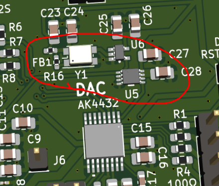
In addition to the ADC and the DAC, I plan on using the following ICs to supply the master frequencies:
- ECS-3225MV-491.52-CN-TR: This is a 49.152MHz clock generator chip.
- SN74LVC1G04: this inverted chip will be used to buffer the clock generator’s output.
- SN74LVC1G74: this flip-flop will be used to divide the frequency for the AK4432.
When choosing these chips, I made sure that they could all switch fast enough for the operating frequency, and could drive each other’s (and the ADC’s/DAC’s) inputs/outputs.
Luckily both chips work at 3.3V, so no voltage translation has to be done.
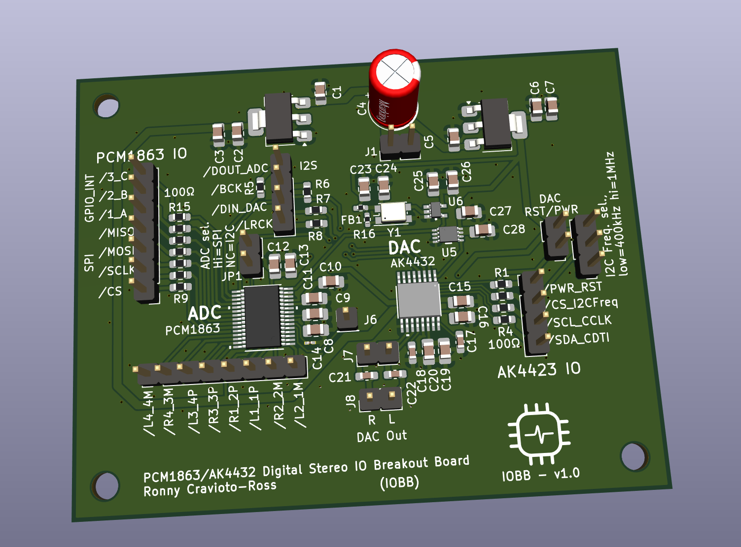
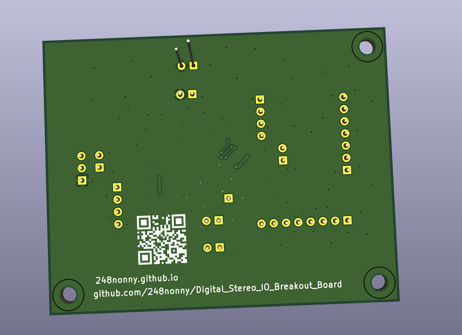
I used KiCAD to create a circuit schematic and PCB design. I added headers for the I2S bus, for the serial communications pins on both the ADC and DAC, and the analog input/output pins. I also made sure to expose the GPIO pins on the ADC, just in case I want to use them later.
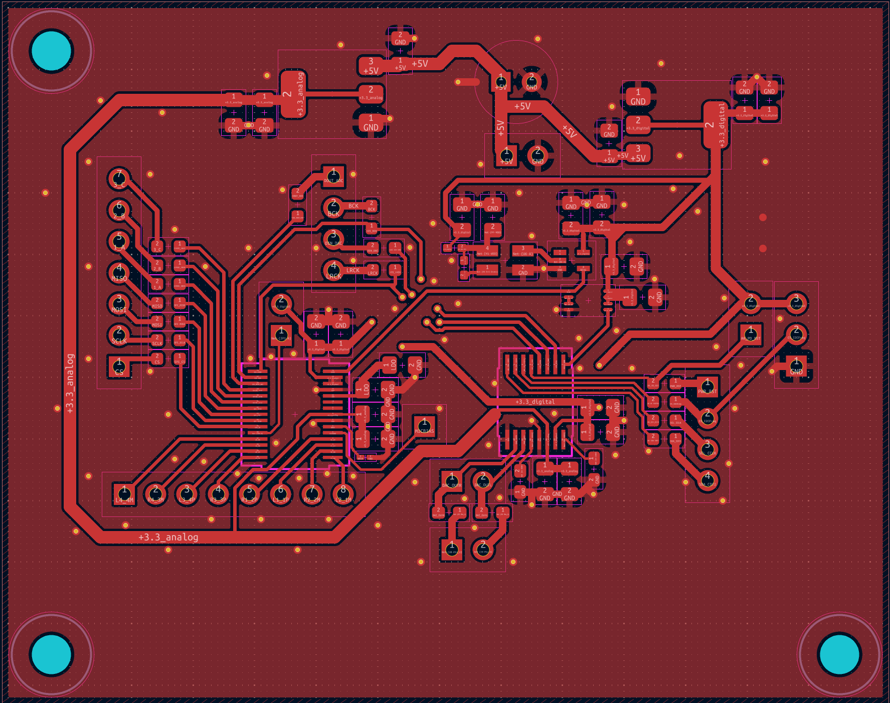
See below images of the PCB design! The KiCAD files can be found on my github.
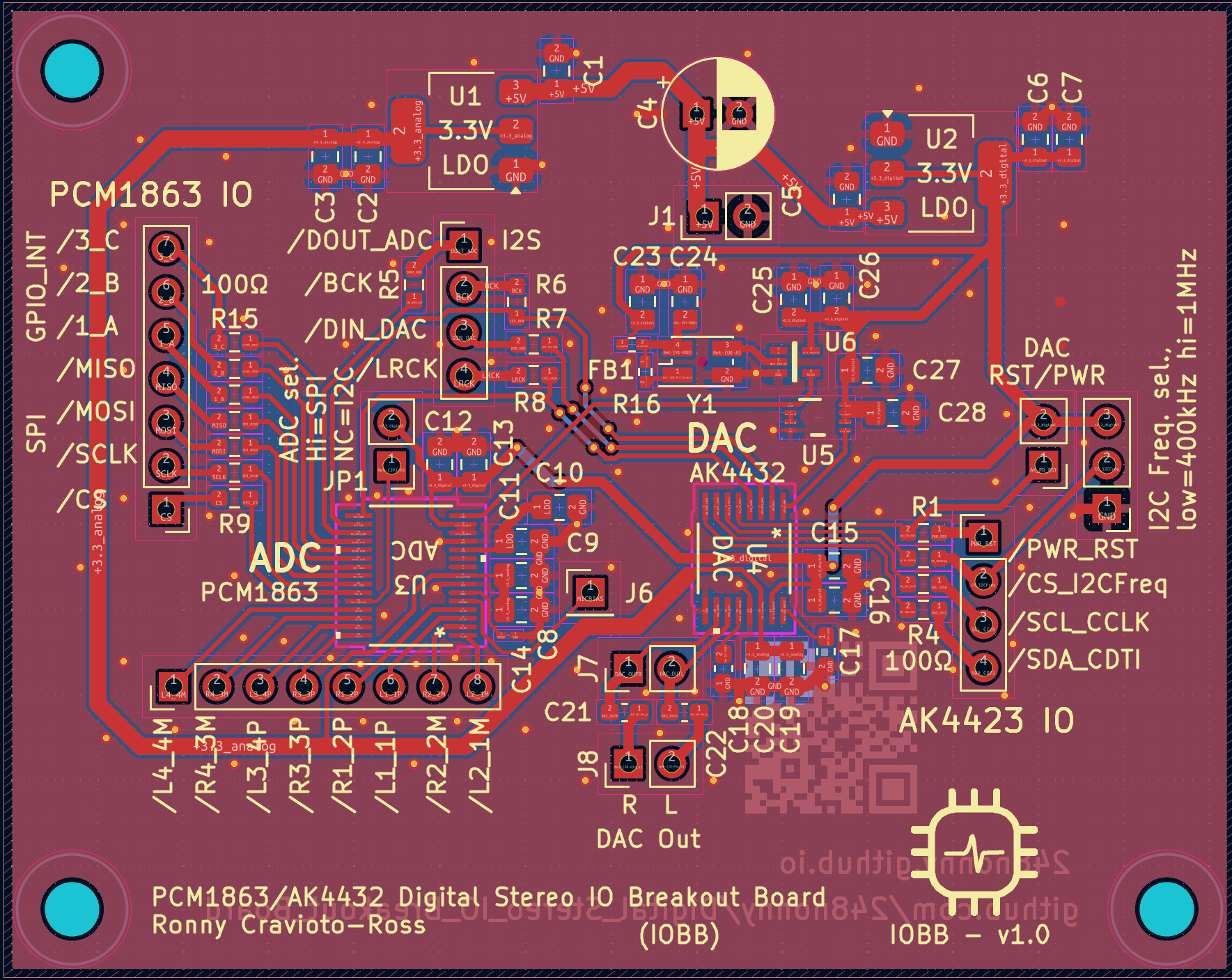
I took some things into consideration for optimal noise performance. Specifically, I made sure that:
- The bottom side was as close to an unbroken ground plane as possible.
- The analog and digital parts of the circuit are separate in the sense that a straight line can divide the analog side of the circuit from the digital side (this avoids noise pickup due to shared ground return paths).
- Plenty of vias were used for ground stitching to the bottom plane.
- Filter/decoupling capacitors (0.1uF and 10uF) are used at every DC power input.
- Separate 3.3V supplies were used for the analog power and digital power pins on the ADC and DAC chips (hence the two separate LDO regulators at the top of the board).
Both the ADC and DAC have different communication modes; both can use I2C or SPI (you can choose between them). Connections to the serial lines are exposed on the headers marked “PCM1863 IO” and “AK4432 IO,” and the four I2S lines are exposed on the center-left header labelled “I2S.” The 8 pin header just below the ADC are the analog input pins (the internal mux can switch between them), and the DAC’s stereo output is exposed (both straight from the chip and through DC filtering caps) on the pins below and slightly left of the DAC.
The three chips used to generate the master clock signal (listed above) are circled in the below image:
The circuit is meant to be powered by the RPi’s 5V power output, and is regulated down to 3.3V by the two separate LDO regulators (seen near the top of the PCB). The 5V input is stabilized by a large 100uF capacitor (seen in red on the CAD rendering).
Conclusion
Overall, the circuit is meant to test the ADC and the DAC with the Raspberry Pi, and as such I tried to keep it as simple as possible. Aside from the clock generator and 3.3V LDOs, the PCB basically just exposes the IC’s pins so that they can be connected to the RPi.
I ordered the PCB already (to Vancouver), and as soon as I get back from my co-op in Lethbridge AB, I’ll get to assembling and testing it!!